AN APPROACH TO ANTENNA TUNING
by
Lloyd Butler VK5BR
Some ideas are presented on how to match the transmitter to the complex impedance of the antenna circuit and an examination is made of the tuning range needed for matching components.
(Orininally published in the journal "Amateur Radio", June 1987)
INTRODUCTION
As a preliminary exercise to designing a new tuner, the writer set out to find out what tuning components would be needed and how they might best be connected. What follows is essentially a paper exercise making use of a computer program to simulate a wide range of tuning conditions. From the results, some interesting curves have evolved leading to a few ideas on tuner application.
The function of the antenna tuner is to transform the complex impedance presented by the antenna, or its feeder system, to a resistive value suitable to load the transmitter. This resistive value (Rs) is normally 50 ohms and throughout the discussion which follows, this value is assumed.
The spread of resistive and reactive components which must be matched depends on the type of antenna system used. Where antennas are carefully matched to transmission lines, the spread is limited, but where feeder lines are tuned, or compromise antenna systems are used, a wide range of values has to be accommodated.
It is difficult to define precisely what range of values might be needed, but the writer initially decided to aim for the following specification:
Frequency Range - bands 1.8 - 28 MHz inclusive.
Resistance Range - 1 to 1000 ohms.
Reactance Range - -1000 to + 1000 ohms.
Peak Power Rating - 400 watts PEP
This turned out to be quite a tall order, not because of any theoretical problem, but because on the low frequency bands, particularly large values of variable inductance and capacitance are required.
|
| |
A MATCHING PRINCIPLE
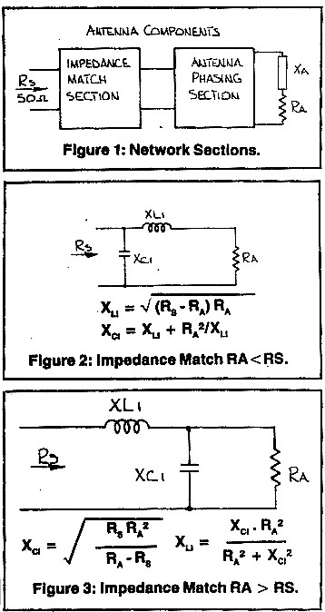
The first approach was to make use of a principle described by the writer in Amateur Radio, December 1985. Referring to Figure 1, a network is made up in two sections, an antenna phasing section which cancels any antenna reactive component and an impedance matching section (often called an L match) which transforms the remaining resistive component to a value equal to Rs (50 ohms).
The L match makes use of the characteristic of a resonant tuned circuit in that the parallel resistance across the circuit is equal to the resistance seen in series with it multiplied by (Q + 1) squared. By making the matching circuit resonant in conjunction with the antenna constants and selecting the L and C components to set the Q as required, the resistive component of the antenna is made to appear larger or smaller at the input of the matching circuit. If the antenna resistance component (Ra) is lower than the required load resistance (Rp), usually 50 ohms, then the antenna is connected in series with the tuned circuit and the transmitter line connected in parallel with it. If the antenna resistance component (Ra) is higher than Rp, then the reverse is connected with the antenna across the tuned circuit and the transmitter line connected in series with it.
There are two reactive components in an L match, one is in series and one is in parallel. One is an inductor and one is a capacitor. Combined with reactance of the antenna, they form the tuned circuit and their values are selected to achieve the required value of loaded Q. . Whether the shunt or series component comes first depends on whether the reflected resistance is to be made greater or lower than Rp. Which of the L or C components goes in series or parallel depends on choice of design - either can be in either place.
The article makes use of some formulae which have been worked out for the L Match by the writer.
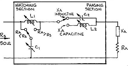
The impedance matching section is illustrated in Figures 2 and 3. Where the load resistance Ra is less than the source resistance Rs, the circuit and formula of Figure 2 is used. In this case, capacitive reactance XC1, is at the input. Where Ra is greater than Rs the circuit and formula of Figure 3 is used. In this second case, capacitive reactance XC1, is at the output.
The antenna phasing section can simply be a series reactance equal, but opposite in sign, to the antenna reactance (Xa), that is, a capacitor to balance inductive reactance, or an inductor to balance capacitive reactance.
|
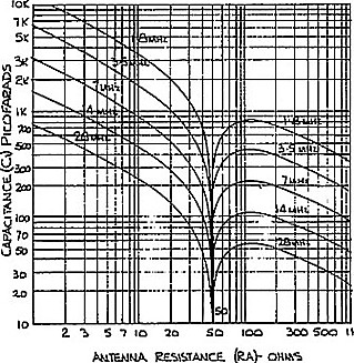
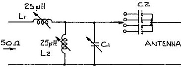
Using the principles described, the tuner as shown in Figure 4 is evolved.
|
|
Figure 4: A Tuning Principle
|
COMPONENT VALUES
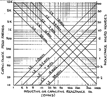
The writer set out to determine the range of values of C1, C2, L1 and L2 in the circuit (Figure 4) over the frequency and impedance ranges previously discussed. As many permutations were required, a computer program was set up to produce tables of results which were used to prepare the curves Figures 5-7. Figure 5 shows the capacitance of C1 plotted as a function of Ra for each of the principal amateur radio HF bands. The figure illustrates the very large capacitance required for low values of Ra, particularly on the low frequency bands. Figure 6 shows the inductance of L1 plotted as a function of Ra for each of the bands.
| |
Figure 5: Matching Capacitance as a Function of Antenna Resistance.
|
|

| |
Figure 6: Matching Inductance as a Function of Antenna Resistance.
|
|
The value of phasing capacitance C2, or phasing inductance L2, can be read off as a function of Xa for each band from Figure 7. The very large value of C2 is also illustrated for low values of antenna inductive reactance (Xa).
|
|
Figure 7 Matching Capacitance or Inductance as a Function of Reactance
|
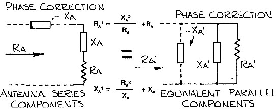
PARALLEL ANTENNA PHASE CORRECTION
The antenna impedance, in the form of a resistive and reactive component in series, can be transformed to two other components of resistance and reactance in parallel, as shown in Figure 8 using the formula included with the diagram.
|
|
Figure 8: Parallel Equivalent of Antenna Circuit.
|
As an alternative to phase correction by series tuning, as shown in Figure 4, the reactive component can be cancelled out by a parallel reactance equal but opposite in sign to the equivalent parallel reactance. This method of phase correction has a number of attractive features as follows:
1. The equivalent shunt reactance is much higher than the series value (Xa) and if the antenna is inductive, a smaller value of phasing capacitor is needed to tune it out. (It does mean, however, that a larger value of Inductance is needed to tune out the reactance of a capacitive antenna).
2. If the tuner is to couple to a balanced circuit, series components must be balanced in each line Ieg and the number of series components is doubled. With parallel tuning, a duplication of components is not required.
3. Referring back to Figure 5, we see that the capacitance required in the matching circuit decreases as the antenna load resistance (Ra) is increased. The effect of parallel tuning is to present a new value of load resistance (RaI) higher than the value of Ra and hence the size of the capacitor in the matching section can be reduced.
On the negative side, the increased antenna circuit impedance does increase the voltage developed for a given power and hence the voltage across the parallel tuning capacitor.
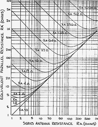
Figure 9 plots the equivalent parallel resistance (RaI) as a function of series resistance (Ra) for different values of series reactance (Xa). Figure 10 plots the equivalent parallel reactance (XaI) as a function of series reactance different values of series resistance (Ra). Figures 9 and 10 are a graphical representation of the formulae shown in Figure 8.
| |
Figure 9: Equivalent Parallel Resistance as a Function of Antenna Series Resistance and Reactance.
|
|

| |
Figure 10; Equivalent Parallel Reactance as a Function of Antenna Series Resistance and Reactance.
|
|
Figure 11 illustrates the application of parallel phase correction. Capacitor C2 combines the function of matching capacitor for RaI > Rs with the function of phase correction for an inductive antenna. Capacitor C1 provides matching for RaI < Rs and is set to minimum for RaI > Rs.
Another idea is to use parallel phase correction for an inductive antenna together with series phase correction for a capacitive antenna, as shown in Figure 12. This gives a lower value of phasing inductance (L2) for the capacitive antenna as well as a lower value of phasing capacitance for the inductive antenna.
Cl - Matches for RaI < Rs
C2 - Matches for RaI > Rs and also balances
out XaI for inductive antenna.
L1 is the matching Inductance.
L2 - Balances out Xa' for capacitive antenna.
| |
Figure 11: Use of Parallel Antenna Phase Correction.
|
|

C1 - Matches for Ra (or RaI) < Rs
C2 - Matches for Ra (or RaI) > Rs and also
balances out XaI for inductive antenna.
L1 - Is the matching Inductance.
L2 - Balances out Xa for capacitive
antenna.
|
Figure 12: Use of Combined Parallel and Series
Antenna Phase Correction
|
|
The curves of Figures 5 and 6 can be used to calculate the matching sections components using parallel antenna phasing with the series antenna resistance (Ra) substituted by equivalent shunt resistance (RaI).
PRACTICAL VARIABLE INDUCTORS AND CAPACITORS
At this point, an examination of practical values of the components will be made. It is one thing to calculate a range of tuning inductance and capacitance but another thing to obtain the components to do the job.
As far as the inductors are concerned, it is not too much trouble to construct 25 to 30 microhenries of inductance suitable for fitting with switchable taps. A value discussed later is 28 microhenries and this can be achieved with 35 turns, one inch radius and spaced to a length of three and a half inches. Inductance can be calculated using Wheeler's formula which follows:
L (microhenries) = (a2N2)/(9a + 10Ln)
where:
a = radius in inches
N = number of turns
Ln = length in inches.
This becomes:
L = (a2N2)/2.54 (9a + 10Ln)
for dimensions in centimetres.
Reference to Figure 6 shows that 28 microhenries is more than sufficient for the matching circuit. Reference to Figure 7 shows that 28 microhenries can phase correct a capacitive antenna of Xa = - 300 ohms at 1.8 MHz and Xa = - 600 ohms at 3.5 MHz.
Considering now the tuning capacitance, its maximum value is considerably restricted by the maximum voltage applied across its plates and hence the necessary spacing of the plates. The larger the plate spacing required, the more difficult it is to achieve a high value of capacitance. Where a capacitor is connected across a resistive load, the voltage developed across its plates is proportionally to the square root of both the load resistance and the power; i.e. E = 1.4√( PR).
When tuned correctly, the capacitor facing the transmitter is across 50 ohms; however the capacitor across the antenna circuit could be facing a much higher resistance particularly if parallel antenna phasing is used. Typical voltages could be as follows:
P = 100W, R = 100 ohms, E PEAK = 140 V
P = 100W, R = 1000 ohms, E PEAK = 442 V
P = 100W, R = 5000 ohms, E PEAK = 990 V
P = 400W, R = 100 ohms, E PEAK = 280 V
P = 400W, R = 1000 ohms, E PEAK = 885 V
P = 400W, R = 5000 ohms, E PEAK = 1980 V
According to ITT Reference Data for Radio Engineers, an approximate rule for uniform fields is that the breakdown gradient of air is 30 peak kilovolts per centimetre or 75 peak kilovolts per inch.
Large values of variable capacitance can be made up using old style receiver tuning gangs. Each section of these usually has a maximum capacitance of about 450 pF making a total capacitance of 990 pF for two gang sections, or 1350 pF for three gang sections. The plate air spacing on these seems to average around 0.01 inch, which on the ITT approximation, has a breakdown voltage of 750. Referring to the curve of Figure 13 (also from the ITT handbook) a slightly higher voltage is indicated providing there are no sharp points to concentrate the field, (possibly 1000 V). Based on this assumption, the receiver type gang could be satisfactory for a 100 W transmitter but could arc over when using higher power (say 400 W from a linear amplifier). Operation in the writer's own radio shack has verified this prediction.
Tuning capacitor plate spacing of at least 0.02 inch would seem necessary to operate 400 W PEP, and for this spacing, suitable capacitors above 200 to 240 pF are difficult to find. A tuner design aimed at reducing the range of capacitance tuning would clearly be an advantage.
|
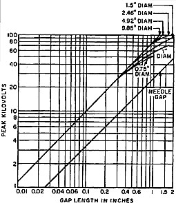 Figure 13: Spark Gap Breakdown Voltages
|
|
REDUCTION OF MATCHING CAPACITANCE
Referring back to Figures 2 and 5, the largest values of matching capacitance are required when Ra is less than Rs, with the capacitance connected at the input of the network. If Ra could be artificially increased above Rs, for all antenna impedance conditions, the need for the input capacitor would be eliminated. Use of parallel antenna phasing results in an increased value of antenna load resistance (RaI) but for low values of Xa, RaI is still lower than Rs.
Examining Figure 9, it can be seen that RaI can be kept higher than Rs by ensuring that Xa is always higher than 30 ohms (or less than minus 30 ohms). This can be achieved by adding lumped reactance to the antenna circuit with an inductor or capacitor.
One circuit simulated on the computer used series capacitance switched by incremented steps into the antenna circuit. For each antenna impedance condition, a capacitance was selected which made the antenna circuit look at least 30 ohms capacitive. For an inductive antenna, the added capacitive reactance was made equal to the inductive reactance plus approximately 30 ohms.
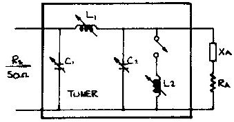
The elements of the circuit are shown in Figure 14. Component bank, C2, is the added series capacitance selected to eliminate the matching circuit input capacitor. Parallel inductance (L2) resonates with the effective antenna shunt capacitance up to the point where the inductance limit of 25 microhenries is reached. C2 has a wide capacitive range but need not be continuous in its coverage, that is, switched fixed capacitors substitute for a prohibitively large variable tuning unit. Switched capacitors, incremented in a ratio of 1.4 to 1, have been found to be satisfactory. Trimming between switched steps is corrected by adjustment of matching capacitor C1. This capacitor also adds extra capacitance to resonate with L2 when L2 has reached its limit of 25 microhenries.
A further circuit is shown in Figure 15, in which the antenna section is made to have at least 30 ohms of inductive reactance, by simply increasing the value of series phasing reactance (L2) until this condition is satisfied. The circuit is, in fact, a development of the principle discussed relative to Figure 12, but with the antenna tuning constants altered to achieve elimination of the input matching capacitor. Only one variable capacitor (C1) is required which combines the function of impedance matching capacitance with that of a capacitance to equalise the shunt reactance reflected across it from the antenna circuit.
Range of capacitance required for C1:
1.8 MHz -- 280 to 900 pf
3.5 MHz -- 80 to 450 pf
7.0 MHz -- 25 to 225 pf
14 MHz -- 13 to 115 pf
28 MHz -- 11 to 57 pf
C2 Fixed capacitance range:
(Capacitors are incremented on steps of 1.4:1).
1.8MHz -- 47 to 4700 pf
3.5MHz -- 30 to 2200 pf
7.0MHz -- 20 to 1500 pf
14.MHz -- 10 to 1200 pf
28.MHz -- 10 to 820 pf
| |
Figure 14: A Circuit with Parallel Antenna Phase Correction and Added Series Capacitance (see text).
|
|

Capacitance range of C1 plus fixed C:
1.8 MHz -- 300 to 2000pf
3.5 MHz -- 150 to 750 pf
7.0 MHz -- 40 - 300 pf
14. MHz -- 20 - 120 pf
28. MHz -- 10 to 50 pf
|
Figure 15: A Circuit with Parallel Antenna Phase Correction and Added Series
Inductance. Only One Variable Capacitor Is Required. (see text).
|
|
Table 1 shows the range of antenna impedances which can be matched and the variation of L and C components needed for each of the main amateur bands. The table is based on a maximum component inductance of 28 microhenries and an effective antenna inductive reactance set at a minimum of 65 ohms at 1.8 MHz. This value of reactance has a considerable effect on the value of all three tuning components and 65 ohms (increasing a little as frequency is raised) works out to give a better compromise for all component values than the 30 ohms originally nominated.
 |
Table 1: Range of Antenna Impedances Tunable and
Range of Inductance and
Capacitance Required for
Circuit of Figure 15.
|
Of course, table 1 is a theoretical conclusion based on simulated conditions using perfect inductors and capacitors. No allowance is made for the effect of loss resistance in the components themselves. (For example, an antenna resistive load of 2 ohms might be considerably increased by the loss resistance of the tuning inductor in series with the antenna).
The range of reactance is not quite as great as that aimed at in the original specification, but as indicated earlier, that specification was a little over ambitious.
To tune up to 1.8 MHz, C1 needs a tuning range to 2000 pF. In the diagram, a variable capacitor with a maximum value of 250 pF has been assumed and three fixed capacitors have been included which can be switched in various combinations to extend the range to
2000 pF.
BALANCED TUNING
If the tuner is to feed balanced lines, a balanced tuner is required. Series components should be split so that half of each component reactance is placed in each balanced line leg. One idea might be to use tapped (and switched) variable inductors with mutual
coupling between the balanced inductor halves, as shown in Figure 16. In this arrangement, the same combined inductance with the same number of combined turns, is achieved as with the single inductance in the unbalanced circuit. The idea is to cut the coil at its centre and connect one half in each line leg, making sure that the sense of connection gives additive and not subtractive combined inductance (refer to Figure 17).
 Figure 16: Balanced Tuner Using Mutually
Coupled Inductance Between Each Leg of
the Balanced Circuit.
Figure 16: Balanced Tuner Using Mutually
Coupled Inductance Between Each Leg of
the Balanced Circuit.
|
|
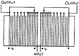 Figure 17: Winding of Balanced Inductor.
|
|
A balun transformer is required to interface the unbalanced transmitter output circuit to the balanced circuit. The primary reactance of the balun should be at least four times the circuit impedance at the lowest operating frequency, (i.e. four times 50 ohms or 200 ohms). At 1.8 MHz, this means a minimum inductance of 17.6 microhenries. A shunt reactance of 200 ohms across the 50 ohm circuit reflects an equivalent series reactance of about 17 ohms (i.e. one microhenry) to the matching circuit. This will affect the matching circuit but only to a minor degree.
The wideband balun transformer is easily constructed, using a tri-filar winding on a suitable toroidal core, selected for the frequency range and with sufficient core cross section area to prevent core saturation.
The minimum number of tri-filar turns is calculated as follows:
Turns(T) 25√( L/AL)
where:
L = minimum primary inductance in microhenries
AL = number of microhenries per 100 turns from manufacturers specifications.
The operating flux density (Bop) is calculated as follows.
Bop = (Erms X 108)/(4.44fNAc) GAUSS
where:
Erms = √(PR = 140V) (for 4OOW in 50 ohms)
f = frequency (Hz)
N = number of turns
Ac = cross-section area of core in square cm.
The flux density should be much lower than the saturation value (about 10 000 gauss for iron powder cores).
A suitable toroid for the high power case is the Amidon T200 (2 Mix Red). Its cross-section area is 1.33 square centimetres and it has an AL factor of 120 microhenries per 100 turns. Twelve tri-filar turns on this core is satisfactory for 1.8 MHz.
One might question why the balun could not be placed at the output of the tuning system allowing the whole system to be unbalanced. The problem here is that the transformer would not only have to be designed for a wide range of frequencies, but it would also have to be made to operate over the wide range of output impedances, a somewhat difficult proposition.
FIXED CAPACITORS
Some care must be taken in selecting fixed capacitors. If high impedance feed systems with high powers are anticipated, voltage ratings in the order of 1500 to 2000 volts should be considered. In high power RF work, voltage is not the only consideration as capacitors made for this purpose are also given a maximum current rating. At low frequencies, voltage is the limiting factor, but the reactance of a capacitor decreases with frequency and hence for a given voltage, current through the capacitor increases with frequency to a point where current is the limiting factor. At the highest operating frequency, the current, calculated by dividing the maximum expected voltage by the reactance, should not exceed the capacitor current rating.
Another factor, particularly relevant to ceramic capacitors, is the need to reduce voltage and current ratings when temperature rises to any extent, due to internal heating of the capacitor. Ceramic capacitors generally have considerable loss resistance which can produce heating of the dielectric when high RF currents are passed through the capacitor.
A possible option for radio amateurs is to acquire high voltage mica capacitors from discarded old radio transmitters.
CONCLUSION
The curves included give a lead to the order of components needed to match the ransmitter to a wide range of antenna impedance loads. On the low frequency bands, the range of tuneable capacitance needed becomes a problem. This range can be reduced by parallel phase correction of the antenna circuit rather than series phase correction.
The circuit, Figure 15, makes use of part series and part parallel phase correction. By enforcing a condition of inductive reactance in the antenna circuit, a single tuneable capacitor element of fairly large (but not intolerable) range is achieved. The circuit of Figure 15 (and perhaps the balanced version in Figure 16) appears to be an attractive proposition for a wide range tuner. Of course, the proof of the pudding is in the eating and it must be emphasised that practical application of the idea has yet to be tried.
A few pointers have been thrown in with the discussion concerning the selection of suitable components. Availability of these is another real problem.
There are all sorts of ways of matching a transmitter to an antenna. What is written here should give some food for thought on this subject.
LATER FOOTNOTE
At the time of writing this article, the writer had not been introduced to the now popular Z Match Tuners which also make use of the L matching principle as described in the article. (Refer to later articles by the writer on the Z Match and in particular the single coil version. A feature of the Z Match circuitry is that it enables adjustment of the inductive reactance element in the L match network by using a variable shunt capacitor connected across a fixed inductance.
If the antenna load resistance (Ra) is lower than the source resistance (Rs), it has been assumed that one must use the circuit of figure 2. However, as a result of experimenting with the Z Match Tuner, it is now clear that if there is series reactance in the output circuit, it can be considered in the equivalent parallel form (see figure 8) and the circuit of figure 3 can be applied. This is how the Z Match (which uses the Figure 3 configeration) can match both high and low resistance loads.
,
REFERENCES
(1) "Loading up on 1.8MHz" by Lloyd Butler VK5BR - Amateur radio, December 1985
(2) "An L of a Network" by Graham Thornton, Amateur Radio, April and May 1995.
Back to HomePage